The Glitch Delay is the Teensy based eurorack Delay module I designed that you can read more about here. The video shows what it sounds like, but I thought I’d go into some more detail about how it actually works, and how I went about designing it.
The Hardware
The brain of the module is the Teensy 3.6. The code running on the Teensy uses the Teensy audio library, and implements a new AudioStream. Because the in-built ADC of the Teensy is used by the audio library, we need another way to read the potentiometers, this duty is performed by the PIC. The PIC reads the pots and communicates the values to the Teensy via I2C (a well supported and fairly simple protocol for inter chip communication). Op-amps are used on both the input and the output to scale voltages up and down. You can find the complete schematic here, but I’ll go into detail on the major sections below. Many elements of this schematic are cribbed/stolen from other open source schematics. I’d highly advise checking out the circuits behind the Music Thing and Mutable Instruments modules whose schematics are all up on GitHub. I’m a relative beginner when it comes to electronics, so it’s highly likely there are elements of this schematic that are not best practice or wrong in some way, feel free to email me with feedback and corrections!
Audio input/output
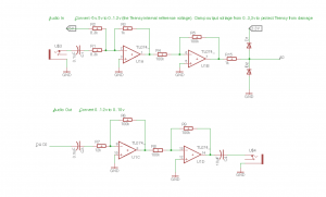
Audio In
The purpose of this section of the circuit it to scale the modular audio signal from (-5V to 5V), into (0 to 1.2V). 1.2V is the voltage of the internal reference in the Teensy. 5V is added to the incoming signal to bias it to be 0V and above. This circuit is an op-amp summing amplifier similar to this.
When Vin = -5V
Vout = ( -(5/8.3) + (-5/8.3) ) = -1.2V (approx)
When Vin = 5V
Vout = ( -(5/8.3) + (5/8.3) ) = 0V
As you can see, this has inverted our signal (the op-amp is in an inverting configuration), so the second op-amp inverts it back again with a gain of 1 (e.g does not change the magnitude of the voltage, it simply inverts the signal)
Audio Out
On the way out we want to do the exact opposite. Scale from (0 to 1.2V) to (-5V to 5V) this is achieved using a simple inverting op-amp.
The gain of the circuit is:
Gain = -(Rf/Rin) = -(100/12) = -8.3
Max voltage from Teensy = 1.2V
1.2 * -8.3 = -10V (approx)
As you can see, this inverts our signal, so the signal is passed through another inverting op-amp with gain 1. The output of this chain will be (0V to 10V) (actually 9.6V, because we are limited by available resistor values). There’s no need to bias, the output capacitor AC couples the output, blocking direct current. Meaning the output signal is centred around 0V, and therefore (-5V to 5V) again.
I found the power line to be quite noisy. I tried using an external voltage reference, instead of the 5V power from the regulator but didn’t notice much improvement. Everything is fine if the gain-staging is sound. However, with very low input volumes/voltages you will hear noise when you amplify the output. In future I would add a trimpot or panel pot to adjust incoming voltage (e.g. R1).
Teensy
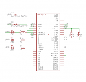
The Teensy’s main duty is to do the audio DSP. It is connected to the PIC chip via I2C. This uses the SCL and SDA pins on the Teensy (with pull-up resistors to the power line). See here for more information. On the Teensy this is supported through the Arduino Wire interface, and is very straightforward. I shall go into more details on the software running on the Teensy in future posts. The Teensy also controls the LEDs and reads the push switches. There are lots of pins on the Teensy, so it seemed best to connect them here. It could have been done with the PIC, but there aren’t enough pins so you’d need to use a multiplexer.
PIC chip
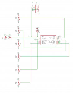
The PIC chip is connected to all the potentiometers. It reads their values and passes the data to the Teensy via I2C. I’ve connected the programming pins to header so it can be programmed on the board. There’s also a connection for an LED for debugging purposes. Neither of these are strictly necessary, but are very useful at the prototyping stage. The capacitor to ground on the power line is as per the data sheet, presumably to deal with minor fluctuations in voltage.
PCB design
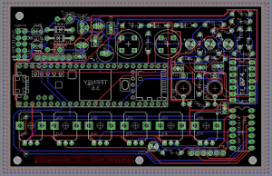
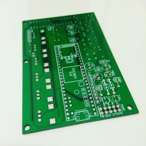
All of this was designed in the free version of Eagle. A very powerful, but rather infuriating piece of software (the UI leaves something to be desired, although is getting better). After you’ve designed the schematic you have to layout the board. This is a fun and at times tricky puzzle game. You need to route all of your connections without crossing over another track on that layer. You can use vias to change to another layer of the board which makes things easier. It’s definitely worth spending some time experimenting to get a layout you are pleased with. You’ll end up with something that looks like this.
You can then send it to a PCB fabrication house to get it made. I used Hackvana, who I was very pleased with. There are a number of alterations I would make on a future board, a major one being that the power connector is too close to the Teensy, meaning I have to improvise a little on the connections. That said, it did work first time, which isn’t bad for a board of this complexity.
In further posts I shall go into a bit more detail about how the software works, and further developments.

Leave a Reply